

WhatsApp Channel Join Now
Telegram Group Join Now
| Relevance: GS Paper III — Science & Technology, Industrial Policy | Source: NITI Aayog Frontier Tech Hub Report, 2026 |
1 · What happened
| A new report by NITI Aayog’s Frontier Tech Hub says India does not yet make enough computer chips (semiconductors) to meet its own demand. This makes our phones, cars and electronics heavily dependent on foreign suppliers.
The report advises India not to chase the most advanced chips right now. Instead, India should focus on simpler chips used in everyday goods, and build large factories at Dholera, Sanand and Morigaon. |
2 · How a Chip Is Made & India’s Game Plan
| A semiconductor fab is a factory that prints tiny circuits on thin discs of silicon called wafers. The wafers are then cut, packed in plastic casings and tested at OSAT/ATMP units before being sold as finished chips. |
|
Institutional Anchor
India Semiconductor Mission
ISM is the central agency that gives money and approvals for chip projects. It has a ₹76,000 crore fund and pays up to 50% of project cost as subsidy.
|
India’s Game Plan
“More-than-Moore”
Skip the most advanced 3–7 nm chips for now. Focus on mature chips (28–110 nm) needed in cars, telecom and industry. Also treat packaging as a main job, not a side task.
|
|
Factories on the Ground
Dholera, Sanand, Morigaon
Dholera (Gujarat): Tata + PSMC ₹91,000 cr fab, 28 nm chips. Morigaon (Assam): Tata’s packing & testing unit, 48 million chips a day. Sanand (Gujarat): Micron, CG Power and Kaynes units.
|
The Hurdles
Slow Build, Foreign Risk
A new fab takes 4–5 years to start, and needs 24×7 power, clean water and ultra-pure chemicals. Most of the world’s chips come from Taiwan and South Korea — any tension there hits India hard.
|
- Design strength: About 1 in every 5 chip designers in the world is an Indian. The Design-Linked Incentive (DLI) scheme aims to push India from just designing for others to creating its own chips.
- Trusted partners: NITI Aayog names the USA, Japan, EU and South Korea as friendly partners for tools and support.
- Market size: India’s chip market is expected to reach $100–110 billion by 2030.
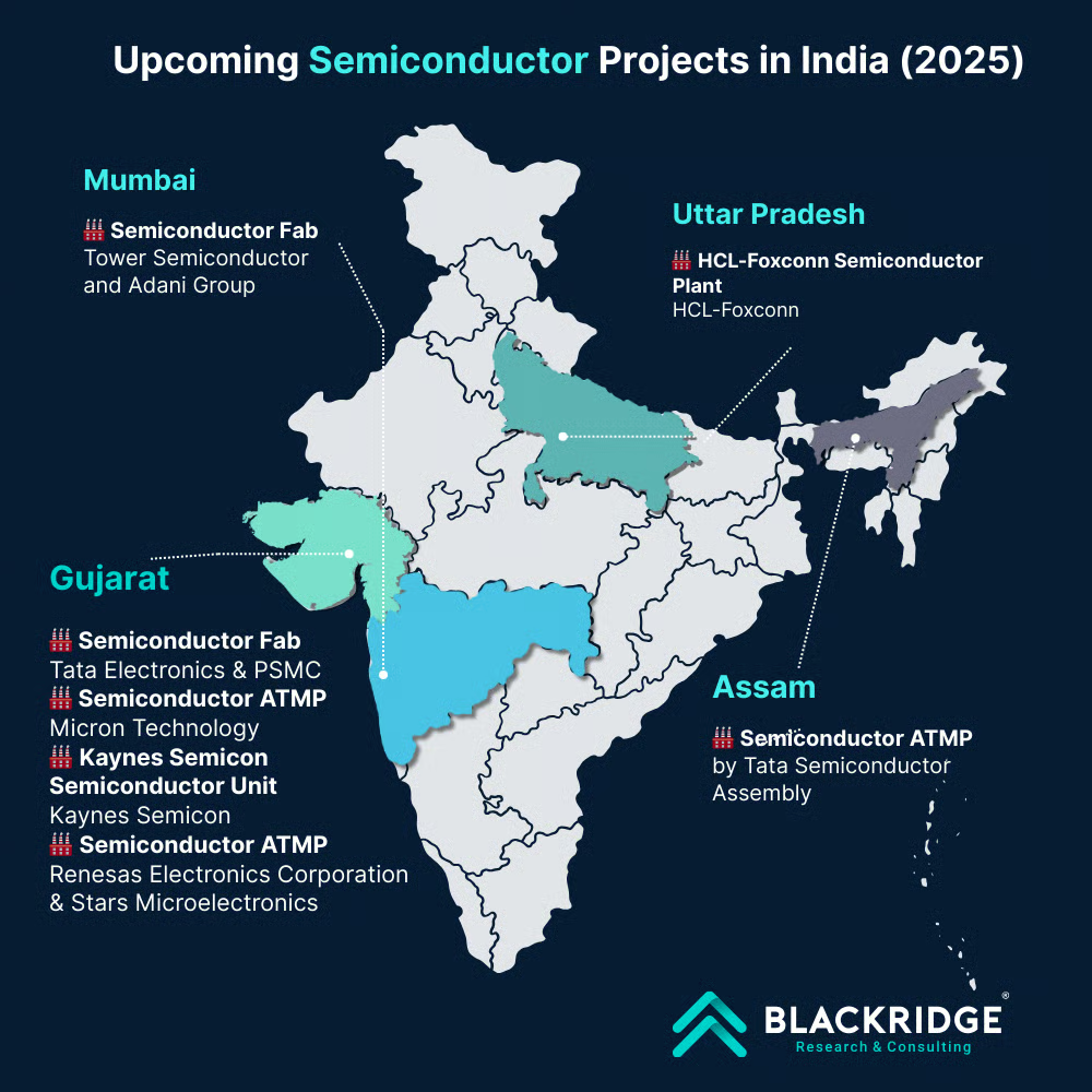
Image: Location Of Semiconductor Plants in India
Note: Moore’s Law is a rule of thumb that says computer power doubles about every two years while getting cheaper. It is named after Gordon Moore, the co-founder of Intel, who noticed this trend in 1965 .
| UPSC Value Box | ||||||||||||||||
|
| MCQ Practice Question |
Q. With reference to India’s semiconductor ecosystem, consider the following statements:
Which of the statements given above is/are correct? |
Answer: (b) 2 and 3 only
|
Share This Story, Choose Your Platform!


Start Yours at Ajmal IAS – with Mentorship StrategyDisciplineClarityResults that Drives Success
Your dream deserves this moment — begin it here.